Importance and Challenges
In the digital era, electronic components are becoming smaller, more integrated, and highly sensitive to electrostatic discharge (ESD). Even a few dozen volts of static electricity can damage ICs, transistors, MEMS sensors, or OLED displays at the nanometer scale. By contrast, a person walking on a nylon carpet can accumulate up to 10,000 V—hundreds of times higher than the 20–50 V threshold that can destroy advanced CMOS transistors.
ESD is a global challenge for the semiconductor industry, producing ultra-short discharges (nanoseconds to microseconds) powerful enough to destroy integrated circuits. Alongside the shortage of semiconductor raw materials, ESD control has become increasingly critical.
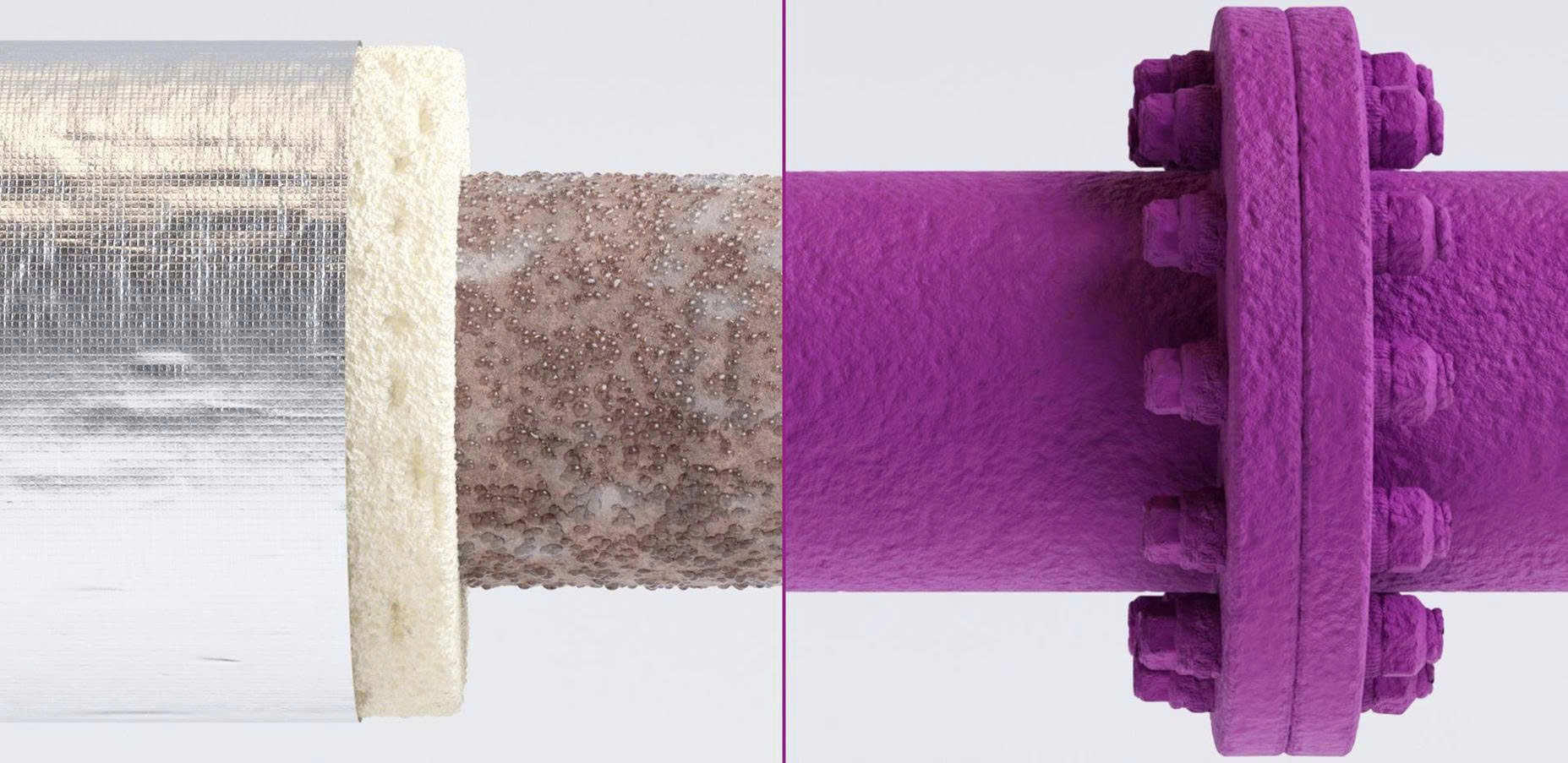
In electronics manufacturing, logistics, and supply chains, ESD films are a key material: they control surface charges, protect components, and maintain essential mechanical properties such as tensile strength, tear resistance, and heat sealability. Major corporations such as Samsung, TSMC, Foxconn, LG Innotek, and Intel enforce strict packaging regulations for ESD, driving worldwide demand for durable, stable, and mass-production-ready ESD films.
The Solution: Anti-Static Packaging Materials
To mitigate ESD, various types of anti-static packaging materials have been developed, including films, trays, tubes, and matrix carriers. Among these, ESD films are the most widely used and are categorized into three main types:
- Conductive – Low resistance, fast electron conduction, channels current through the film rather than the component, capable of handling strong discharges.
- Dissipative – Slows and controls electron flow to the ground; absorbs moisture to form a thin water layer, reducing charge buildup.
- Anti-static – Prevents triboelectric charging caused by contact and separation of surfaces; extensively used in aerospace to protect sensitive equipment.
Beyond electronics and semiconductors, ESD films are also widely used in the food, medical, and aerospace sectors.
Theoretical Basis: Charging, Discharging, and Limitations of Traditional Materials
- Charging mechanism: When two surfaces come into contact and then separate (triboelectric effect), charges accumulate and may discharge once the breakdown threshold is reached.
- Traditional materials and limitations:
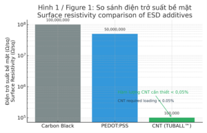
- Carbon black: requires 15–20% loading to achieve <10⁹ Ω/sq → loss of transparency, reduced mechanical strength, and poor processability.
- Ionic salts: rely heavily on humidity, easily washed away, with only short-term effectiveness.
- PEDOT/PSS: transparent conductive polymer, but expensive, unstable under heat/humidity, prone to degradation, and can corrode metal electrodes.
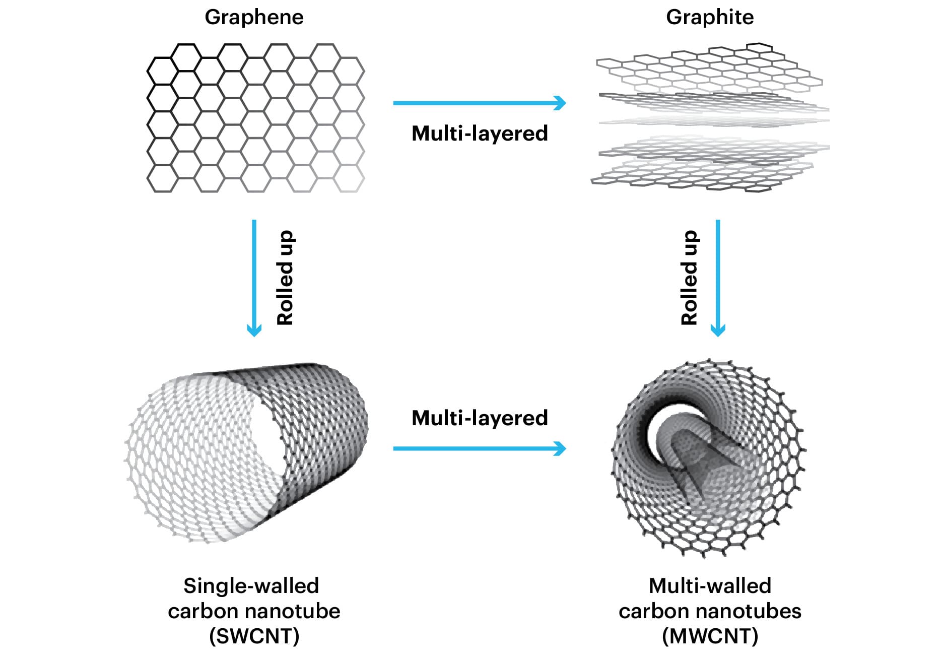
SWCNT (OCSiAl) – Mechanism and Advantages
Single-Wall Carbon Nanotubes (SWCNTs), particularly TUBALL™ by OCSiAl (Luxembourg), have proven to be a superior alternative.
- 3D Percolation Mechanism: CNTs are rolled graphene sheets with nanometer-scale diameters and micrometer-scale lengths. When evenly dispersed in polymers, as little as 0.01–0.05% CNT forms a 3D conductive network, effectively controlling surface charges.
- Key Advantages:
- Ultra-low dosage → saves material, reduces cost.
- High transparency → ideal for optical packaging and display applications.
- Superior mechanical strength → improved tensile and tear resistance while maintaining heat sealability.
- Long-term stability → not humidity-dependent, resistant to washout, effective for years.
- Broad compatibility → easily incorporated into PE, PP, PET, TPU, EVA.
Comparison: SWCNT vs. Carbon Black & PEDOT/PSS
| Criteria | Carbon black | PEDOT/PSS | SWCNT (OCSiAl) |
| Surface resistivity (Ω/sq) | 10⁸–10⁹ (15–20%) | 10⁶–10⁸ (2–5%) | 10⁶–10⁸ (0.01–0.05%) |
| Transparency | None | Moderate | High |
| Mechanical strength | Strongly reduced | No improvement | Enhanced |
| Humidity/thermal stability | Moderate | Low | High |
| Cost–performance ratio | Low, inefficient | High, difficult to apply | Balanced, superior |
Case Studies and Emerging Applications of CNTs
- Samsung: Applied CNT films in OLED and camera IC packaging → improved yield rates.
- TSMC: Integrated CNTs into wafer logistics → reduced ESD-related damage.
- Foxconn: Adopted CNT films for iPhone component packaging → fewer ESD defects, lower inspection costs.
- LG Innotek: Developed CNT + PET films for camera sensor protection.
- Intel: Applied CNT packaging for next-generation CPUs and GPUs.
Emerging applications of CNT ESD films:
- Biopolymer packaging (PLA, PHA, PBAT) → eco-friendly solutions.
- Batteries and EVs → CNTs as conductive additives for separators and electrode coatings.
- Aerospace and automotive composites → CNT films with fiberglass/carbon fiber for enhanced safety and durability.
Single-Wall Carbon Nanotubes (SWCNTs), especially TUBALL™ by OCSiAl, represent a superior ESD protection solution compared to traditional technologies, thanks to ultra-low loading levels, high efficiency, long-term stability, and an excellent cost–performance balance.
Mercury Chemical Co., Ltd., the official distributor of OCSiAl in Vietnam, is committed to delivering advanced SWCNT solutions, supporting enterprises in the electronics, logistics, and energy industries.